 |
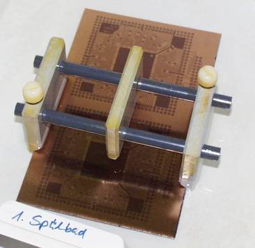
The hand drawn layout then was printed to a inkjet film with a high resolution inkjet printer (HP DeskJet 890C) and then was used as mask for the photographic process of photopositive board material. After developing the photopositive surface, the board looked like in the picture on the left. |
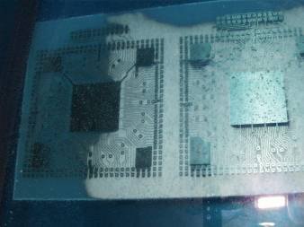 |
The developed board now was put into acid which removes the unused copper of the board. The remaining copper are the signal and power lines used for this CPU board. The photo on the left illustrates this process. You can see that the left part of the board has already a good line structure. The bright parts still are copper and the dark/transparent parts are the blank epoxy-board. |
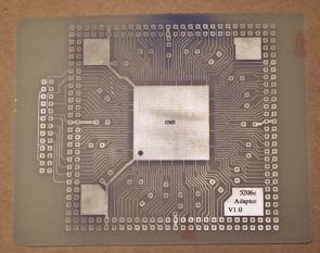 |
This photo is a picture of the finished, undrilled board. Its line-color is silver-white because I have given it for some hours into a bath of gloss tin ("Glanzzinn") which protects the raw copper from oxidation. |
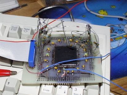 |
Yes! And this picture is a photo of the soldered and finished board! You also see a lot of "flying resistors" in the air, this is because I tested the CPU without any peripherials! This is possible because the ColdFire has 8kB on-chip RAM and allows control over a debug cable. This BDM-cable is connected (the flatband-cable on the left) and enables me to configure the single CPU and let run programs on it! |
| This is the print version. Back to normal view |