The current page has been visited 24096 times.
Visitors today: 4
Hits to all pages: 8179193
Server-Time: 18:24
2024-04-24
|
The ppQBox mainboard
1999-03-21
On Saturday, 1999-03-13, I finished the ppQBox mainboard. Now (1999-03-21) I have the needed
time to update the QBox section to show you the results. The name "ppQBox" (pre_pre_QBox)
I have choosen, because I think I will need two further generations of mainboards before I'm able to
create the "all-killing super-machine" ;) - the real QBox...
1. Images of the board
1.1 Top side view
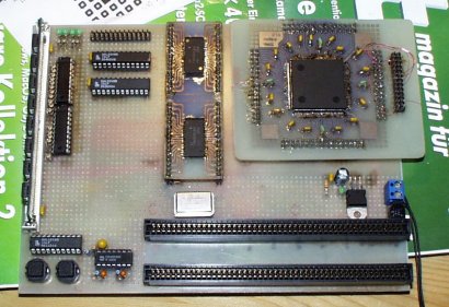 |
This is the top-view of the ppQBox mainboard. Isn't it a nice board?!? ;)
Well, as you can see, the ppQBox consists of three boards: the mainboard, the SRAM board and
of the CPU board. If I get the chance to produce multi-layer boards, it will be of course
only one board but I unfortunately have no chance to do so.... :(
|
1.2 Bottom side view
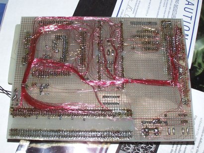 |
Hehehe... and this is the bottom-view of the board... crazy, isn't it? ;) Hmm... I used
the incredible amount of 100 m vero wire... well, and I had much luck: I made
no mistake and the board worked immediately!!! |
2. Functional areas of the ppQBox mainboard
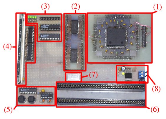
- (1) CPU-Board equipped with a XCF52064FT54 and BDM debug connector
- (2) High-speed SRAM, with GoldCap voltage buffer under the SRAM-board
- (3) Fast parallel network interface built with two GAL20V8, there are also some free IO-lines which drive the four LEDs and give chance for future enhancements.
- (4) PS/2 DRAM, the main memory - of course also EDO-RAM >=60ns. I can use any size of PS/2 RAM with this slot.
- (5) Reset-logic, reset-button and a currently unused signal-button.
- (6) Two expansion slots were all important signals for further hardware add-ons are available. If I need it, I can add also a PCI-Interface to one of the slots... ;)
- (7) 32MHz Quartz Oscillator, free choosable between 0Hz and 50MHz.
- (8) +5V power supply (the 3,3V-supply is under the CPU board!)
3. Discussion / Explanation
The ppQBox mainboard is more or less a standard ColdFire design, I have not much own logic on it.
But this is not really important, the most important step was and is to have a own mainboard,
no more Motorola developer board. The reason for this is, that this way I have the complete control/knowledge
for/about this CPU also from hardware point of view. The Motorola developer board is great to make first steps
with the ColdFire architecture because all works fine immediately. But if you want (like me) to build your own
computer system, you should not rely on ready-to-use example designs...
The main advantage of my mainboard design is the GoldCap buffered SRAM. This option gives me the chance to
have the systems BIOS in a memory which doesn't need to have it's own programming algorithms like FlashROM,
because my memory is a simple SRAM which holds it's data in the power-off mode by buffering the supply voltage
with a 1 F GoldCap.
The two expansion slots mounted on the mainboard are connected to all signals of the address-bus, data-bus and to
all further control lines of the ColdFire/Board. Because of this, the two slots allows me to add almost anything
two the board.
On power-on the following happens:
- The reset logic GAL (see (5)!) asserts a master reset to the complete board including the ColdFire.
- The global chip-select /CS0 is always activated by the CPU if an access to an external address happens.
The SRAM is connected to /CS0 so the ColdFire will start to read the first 8 bytes of data (offset $00000000) from RAM.
These two longwords are the initial stack pointer and the initial program counter, the ColdFire loads the according
registers with the read values.
- Now, the ColdFire continues with command execution on the new program counter. The program at this location is a sort of BIOS,
which sets up anything needed for a full-running system. First, it initializes the DRAM-controller to activate the
PS/2-DRAM, next it programs /CS1 for the Network-IO-GALs, then it changes /CS0 to be on a new position.
- Now, the system is "booted" and the BIOS routine calls the CPU to execute a user program.
You now may ask: "How do you get the code (BIOS) into the unprogrammed board??" -- Well, that's really easy: I use the
BDM-Debug Interface-Cable connected to my PC where I can change everything I need for a initial setup. This setup is only needed
once because all of the next power-on's are fully controlled (without needing a PC!!) from the BIOS located in
the GoldCap-buffered SRAM... ;)
Hmm... that's all for now.
Any comments/questions? Just write a mail to me... :)
|
|


